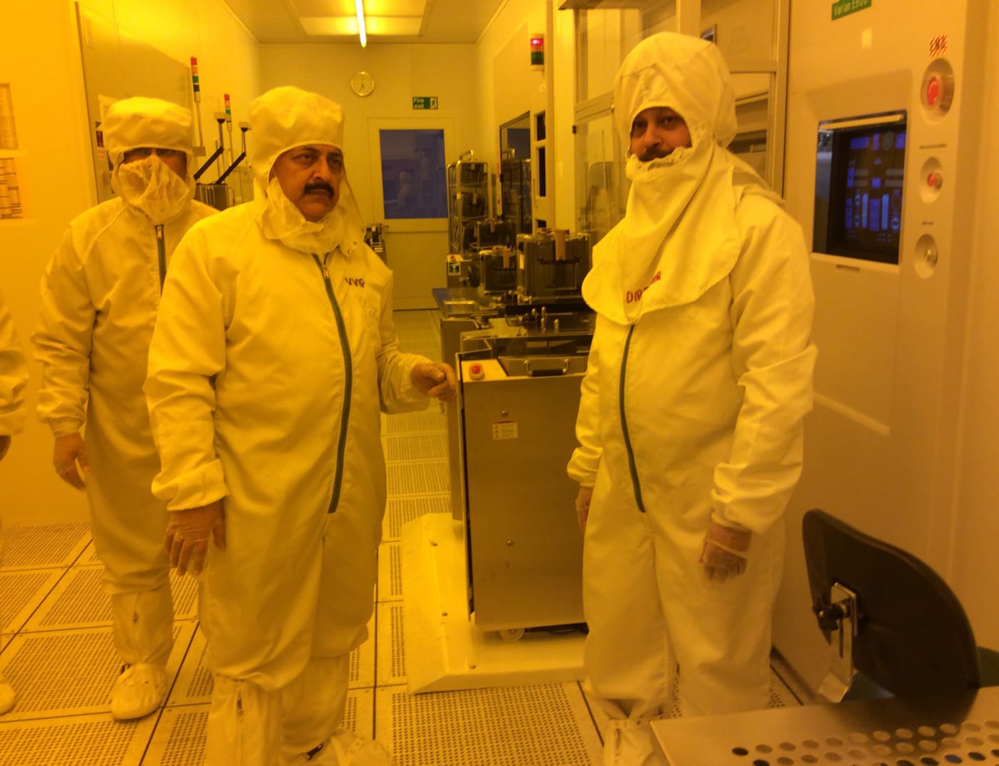
There is a particular shade of yellow that means you are standing in a semiconductor fab. It is not decoration. Photoresist — the light-sensitive coating that lets a circuit pattern be printed onto a silicon wafer — reacts to blue and ultraviolet light, so the whole room is lit with lamps that emit neither. Every chip fab on earth glows the same amber.
Until recently, India had exactly one room like that: the Semiconductor Laboratory at Mohali, a government facility built in the 1980s, making chips for space and strategic use rather than for the market. It was not nothing. But for a country that designs a large share of the world's chips and consumes a rising share of them, one non-commercial fab was a strange gap — and a well-known one. India had tried before. Proposals came and went in 2007, in 2013, in 2017. Each time, the deal collapsed.
So when the India Semiconductor Mission launched in December 2021 with ₹76,000 crore and an offer of up to 50% capital support, the reasonable response was scepticism. Chip fabs are among the most expensive and least forgiving factories humans build. They take years. They need water of a purity most cities cannot supply, power that never flickers, and a supply chain of gases and chemicals that has to arrive on schedule for a decade. Plenty of governments have announced them. Fewer have opened them.
Five years on, here is where it stands.
What has actually been built
Twelve projects were approved under the first phase of the mission. Three of them are in commercial production — a figure the Ministry of Electronics and Information Technology confirmed in August 2026. That is the sentence that matters, because it is the one that could not have been written in 2024.
The sequence went like this:
2023 — Micron, Sanand. A $2.75 billion assembly-and-test plant in Gujarat, the mission's first big investment to break ground. Not a fab: this is the back end of the industry, where finished wafers are cut, packaged and tested. Less glamorous than fabrication, and the sensible place to start — it needs less exotic infrastructure and it builds the workforce a fab will later need.
2024 — Dholera. The ₹91,000 crore Tata–PSMC plant, India's first commercial wafer fab, designed for 50,000 wafers a month. This is the hard one.
2025 — first commercial chips. Kaynes Semicon shipped chips produced commercially in India. Several more fabs and packaging units were approved in the same year.
2026 — Micron Sanand inaugurated. India's first operational packaging plant of the mission cycle opened. Dholera is targeting its first silicon.
Approved chip investment across the mission now stands at roughly ₹1.6 lakh crore.
The part nobody photographs
Fabs get the headlines. The quieter half of the mission is design, and it is where India was already strong — a very large share of the world's chip design engineering has been done out of Bengaluru, Hyderabad and Noida for two decades, for foreign companies, on foreign payrolls.
The mission went after that asymmetry directly. State-of-the-art design tools — the software licences that cost more than most start-ups can raise — have been provided to 332 academic institutes and 105 start-ups. Twenty-four start-ups have been approved under the Design Linked Incentive scheme. The bet is that if an engineering student in Trichy can use the same tools as an engineer at a multinational, some of them will design chips for Indian companies instead of only working on someone else's.
This is cheap policy compared with a fab, and its results will take longer to show. It is also the part most likely to still be paying off in 2040.
What is still ahead
Three things are worth saying plainly, because a site that only prints good news is not worth reading.
India is not making advanced logic chips. Dholera is a mature-node fab. That is the right choice — mature nodes are where the volume is, in cars, appliances, industrial control and power electronics — but nobody should confuse it with the leading edge. The machines that print the most advanced chips come from one company in the Netherlands, and there are not many of them in the world.
The supply chain is still imported. Ultra-pure gases, specialty chemicals, photoresists, the masks themselves — the mission has approved plants for some of these, but a fab in Gujarat currently depends on shipments from Japan, Korea, Taiwan and Europe. Resilience is the stated goal; it is not yet the reality.
Three of twelve is three of twelve. Nine approved projects are not yet in commercial production. Some will slip. Some may not happen. That is normal for industrial policy at this scale, and it is the reason to count operating plants rather than announcements.
Why the world is showing up
SEMICON India 2026, in New Delhi from 17 to 19 September, is the fifth edition of an event that was a modest affair when it started. This year it has 500-plus exhibitors, 240-plus international companies, delegations from more than 40 countries, and six national pavilions — including one from the Netherlands, home of the company that makes the lithography machines.
That last detail is the clearest signal in the whole programme. Equipment makers do not book floor space where nothing is being built. They go where the purchase orders will be.
The Union Cabinet has since approved Semicon 2.0, a second phase built on six pillars. India Semiconductor Mission's chief executive framed the reason in two numbers at the launch press conference: global semiconductor demand is expected to roughly double, from about $1 trillion to $2 trillion, and India's own from about $100 billion to $200 billion. A country that imports nearly all of that has an obvious interest in making some of it.
Where this goes next
Five years is not long in this industry. Taiwan took decades. Korea took decades, with a level of state direction India has not attempted.
What India has done is convert a long record of failed announcements into three operating plants, a wafer fab under construction, a design-tools programme reaching hundreds of institutions, and enough credibility that the global industry now holds one of its annual gatherings in Delhi. Whether that becomes a real supply chain or stalls as an assembly hub depends on the next five years, not the last five.
The yellow rooms are being built. That part is no longer a plan.
See the Semiconductors timeline and sources →
Sources: PIB: India's Biggest Semiconductor Event to be held in Yashobhoomi, New Delhi from 17th – 19th September 2026 (project counts, design-tool and DLI figures, exhibition figures, demand projections) · India Semiconductor Mission, MeitY · SEMICON India 2026 (official) · Timeline and investment figures: India Unfolding